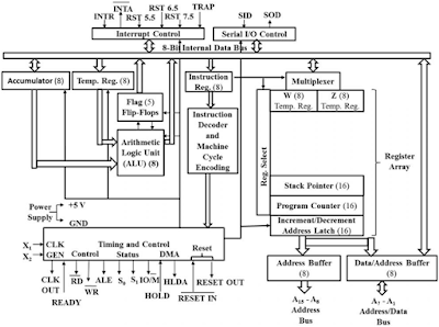
Microprocessor architecture.
- The architecture of microprocessor 8085 can be divided into seven parts as follows:
Register Unit:
General Purpose Data Register
- 8085 has six general purpose data registers to store 8-bit data.
- These registers are named as B, C, D, E, H and L as shown in fig. 1.
- The user can use these registers to store or copy a data temporarily during the execution of a program by using data transfer instructions.
- These registers are of 8 bits but whenever the microprocessor has to handle 16-bit data, these registers can be combined as register pairs – BC, DE and HL.
- There are two internal registers – W and X. These registers are only for internal operation like execution of CALL and XCHG instructions and not available to the user.
Program Counter (PC)
- 16-bit register deals with sequencing the execution of instructions.
- This register is a memory pointer.
- Memory locations have 16-bit addresses which are why this is a 16-bit register.
- The microprocessor uses this register to sequence the execution of the instructions.
- The function of the program counter is to point to the memory address from which the next byte is to be fetched.
- When a byte (machine code) is being fetched, the program counter is incremented by one to point to the next memory location.
Stack Pointer (SP)
- SP is also a 16-bit register used as a memory pointer.
- It points to a memory location in R/W memory, called the stack.
- The beginning of the stack is defined by loading 16-bit address in the stack pointer.
MUX/DEMUX unit
- This unit is used to select a register out of all the available registers.
- This unit behaves as a MUX when data is going from the register to the internal data bus.
- It behaves as a DEMUX when data is coming to a register from the internal data bus of the microprocessor.
- The register select will behave as the function selection lines of the MUX/DEMUX.
Address Buffer Register & Data/Address Buffer Register
- These registers hold the address/data, received from PC/internal data bus and then load the external address and data buses.
- These registers actually behave as the buffer stage between the microprocessor and external system buses.
Control Unit:
- The control unit generates signals within microprocessor to carry out the instruction, which has been decoded.
- In reality it causes connections between blocks of the microprocessor to be opened or closed, so that the data goes where it is required and the ALU operations occur.
- The control unit itself consists of three parts; the instruction registers (IR), instruction decoder and machine cycle encoder and timing and control unit.
Instruction Register
- This register holds the machine code of the instruction.
- When microprocessor executes a program it reads the opcode from the memory, this opcode is stored in the instruction register.
Instruction Decoder & Machine Cycle Encoder
- The IR sends the machine code to this unit.
- This unit, as its name suggests, decodes the opcode and finds out what is to be done in response of the coming opcode and how many machine cycles are required to execute this instruction.
Timing & Control unit
- The control unit generates signals within microprocessor to carry out the instruction, which has been decoded.
- In reality, it causes certain connections between blocks of the microprocessor to be opened or closed, so that the data goes where it is required and the ALU operations occur.
Arithmetic & Logical Unit:
- The ALU performs the actual numerical and logical operation such as ‘add’, ‘subtract’, ‘AND’, ‘OR’, etc.
- ALU uses data from memory and from accumulator to perform the arithmetic operations and always stores the result of the operation in accumulator.
- ALU consists of accumulator, flag register and temporary register.
Accumulator
- The accumulator is an 8-bit register that is a part of ALU.
- This register is used to store 8-bit data and perform arithmetical and logical operations.
- The result of an operation is stored in the accumulator.
- It is also identified as register A.
Flags register
- Flag register includes five flip-flops, which are set or reset after an operation according to the data conditions of the result in the accumulator and other registers.
- They are called zero (Z), carry (CY), sign (S), parity (P) and auxiliary carry (AC) flags; their bit positions in the flag register are shown in fig.
- The microprocessor uses these flags to set and test data conditions.
Interrupt Control
- The interrupt control unit has 5 interrupt inputs TRAP,RST 7.5, RST 6.5, RST 5.5 & INTR and one acknowledge signal INTA.
- It controls the interrupt activity of 8085 microprocessor.
Serial IO control
- 8085 serial IO control provides two lines, SOD and SID for serial communication.
- The serial output data (SOD) line is used to send data serially and serial input data line (SID) is used to receive data serially.

